Semiconductor and biomedical devices
Automating Inspection of Biomedical Wafers
A probing station that images thousands of electrodes and measures test structures, while staying fully usable for R&D.
The problem
A manufacturer of silicon wafers for biomedical devices needed to verify the quality and repeatability of its process. That meant imaging thousands of electrodes for defect analysis, and stepping a probe card through test structures to take electrical measurements.
What we built
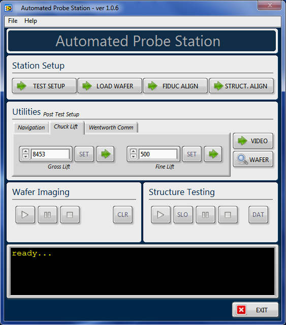
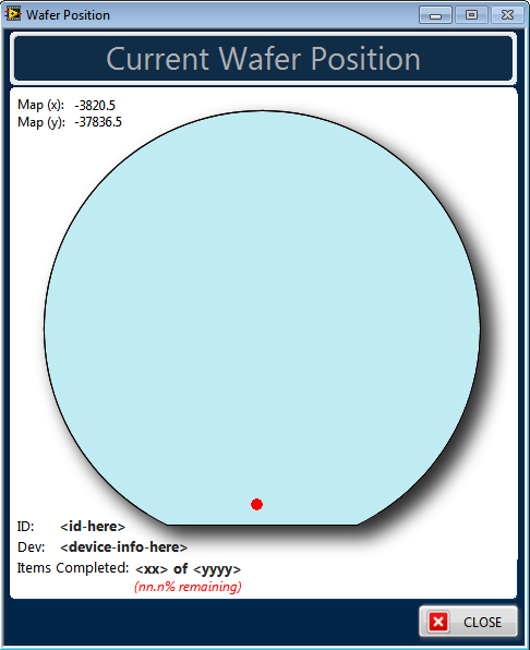
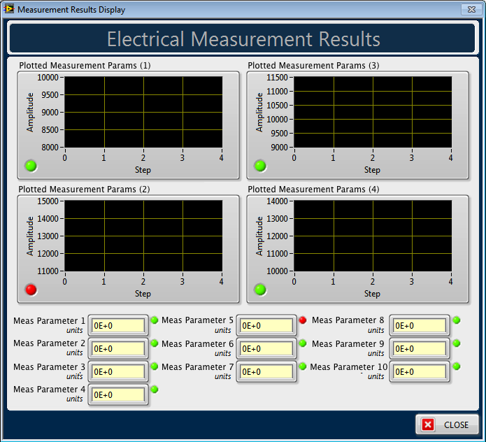
Pre-loaded definition files tell the station where every device sits on the wafer. The application moves a Wentworth Pegasus prober through those locations, streams high-resolution images to disk in a structured way, and runs V-I measurements through Keithley instruments and a multiplexer.
That took custom LabVIEW drivers for the prober over GPIB and for the microscope over RS-232, plus changes to the frame grabber’s supplied driver.
The result
The station works as a production test system, and still gives engineers almost full manual control for diagnostics and R&D.
- LabVIEW
- GPIB
- RS-232
- Keithley instruments
- Frame grabber